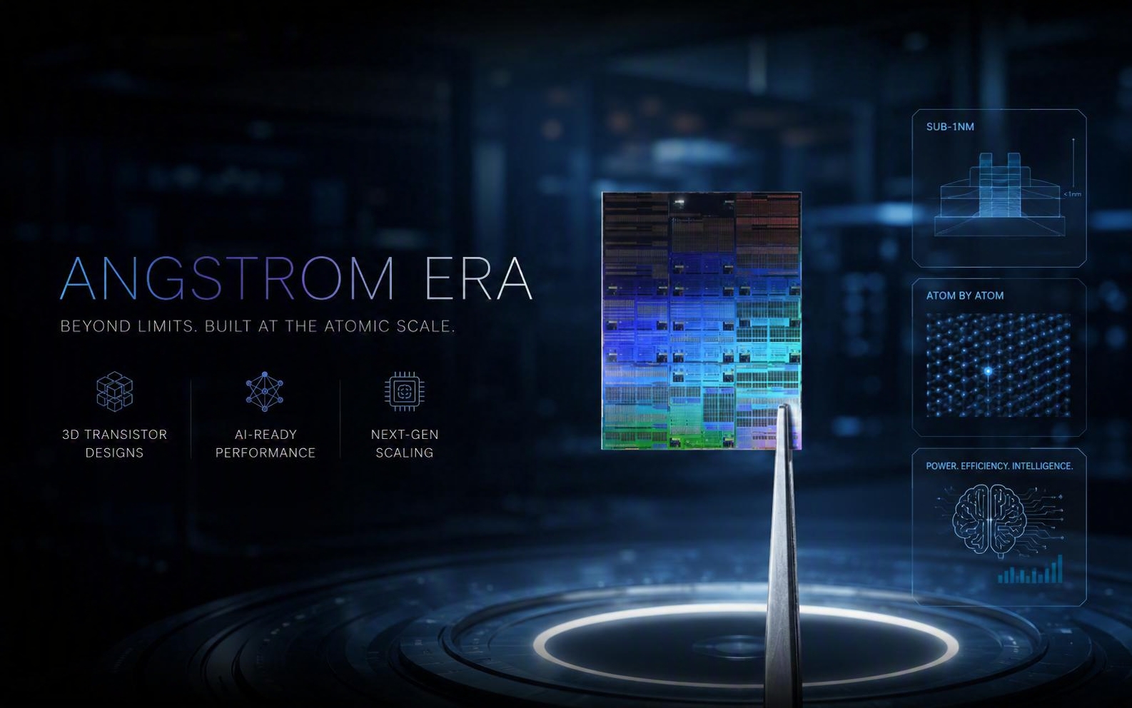

Scaling Beyond Silicon: The Angstrom Era
The global semiconductor industry has officially entered a mind-boggling new era of physical scaling. Recently, researchers cracked physical limits by introducing the first functional Sub-1 Nanometer Chip. This experimental processor marks a historic triumph over the looming threat of atomic leakage. Indeed, the achievement demonstrates that Moore’s Law will survive through pure structural innovation. Future consumer electronics will achieve unprecedented processing speeds within extremely compact dimensions. Specifically, this device opens exciting new possibilities for sovereign personal applications.
Before this breakthrough, experts feared that quantum tunneling would halt further scaling of silicon. Consequently, scientists had to reinvent transistor geometry to continue advancing computing power. Standard horizontal layouts can no longer prevent electrons from escaping their conduction channels. Therefore, vertical stacking has become the primary path forward for advanced chipmakers. This physical transition marks the official beginning of the long-awaited angstrom era. Early tests already show massive leaps in overall speed and electrical efficiency.
The rapid rise of artificial intelligence has created an insatiable demand for powerful processors. Meanwhile, traditional silicon architectures are struggling to meet these intensive compute requirements. These challenges compel industry leaders to invest heavily in advanced vertical designs.
Commercializing the Sub-1 Nanometer Chip
At the heart of this revolution lies a radical shift in transistor design. To achieve this, IBM’s 0.7-nanometer prototype relies on a vertical architecture. The industry calls this pioneering approach the three-dimensional nanostack design. It vertically stacks and staggers field-effect transistors using sequential integration. Consequently, this vertical stacking method effectively doubles the density of components.
The prototype packs nearly one hundred billion transistors onto a fingernail-sized piece of silicon. This incredible density enables much shorter electrical paths inside the processor. With shorter paths, signals travel faster while consuming a fraction of the usual power. This architecture restarts static random-access memory scaling after a twelve-year stall. Indeed, the prototype delivers an impressive forty percent scaling in memory density.
Additionally, this vertical integration lets engineers optimize different channel materials independently. For example, the design can incorporate atomically thin transition metal dichalcogenides. These two-dimensional materials replace conventional silicon to minimize heat and electron leakage. Subsequently, these alternative channels sustain logic scaling down to the angstrom era. In this manner, the combination of new geometries and materials will sustain the roadmap.
Structural Merits of the Sub-1 Nanometer Chip
Leading semiconductor foundries are aggressively updating their long-term fabrication roadmaps. In Taiwan, TSMC is currently building advanced facilities for its upcoming nodes. Specifically, the Taiwanese giant schedules trial production for its sub-one-nanometer A10 node in 2029. This aggressive timeline aims to secure a dominant position in the high-performance computing market. Due to these plans, major tech firms are already placing early orders for wafers.
Meanwhile, Samsung has formed a dedicated team targeting one-nanometer mass production by 2029. This ambitious roadmap relies on a unique forksheet transistor design for tighter cell packing. Similarly, Intel is looking beyond its upcoming fourteen-angstrom process under CEO Lip-Bu Tan. The American chipmaker has officially initiated early development on its ten-angstrom and seven-angstrom nodes. To achieve this, the company is preparing its global foundry facilities for a multi-generational pipeline.
Moreover, Japan’s state-backed Rapidus is racing to bridge the technology gap with industry leaders. The newcomer plans to start trial production of its own one-nanometer node in late 2029. These synchronized efforts signal an intense multi-national race toward the physical limits of silicon. In addition, each company must solve major challenges regarding production yield and thermal management. Ultimately, the successful commercialization of these nodes will redefine global computing capabilities.
Global Foundry Roadmaps and Industry Action
To manufacture at this atomic scale, chipmakers depend heavily on next-generation lithography tools. Specifically, imec received ASML’s advanced high-numerical aperture extreme ultraviolet scanner in March 2026. This massive tool is central to the European Union’s NanoIC pilot line in Belgium. The system enables ultra-precise circuit printing to define features smaller than two nanometers. In fact, the tool will play a pivotal role in accelerating advanced semiconductor research.
However, these expensive machines sit at the center of escalating geopolitical tensions. The Dutch government recently joined the American-led Pax Silica alliance in June 2026. Consequently, ASML faces strict export controls on its advanced deep and extreme ultraviolet tools. This regulatory barrier directly restricts the shipment of critical manufacturing equipment to Chinese buyers. In this environment, geopolitical alignments are actively carving new lines across the global supply chain.
Thus, regional supply chain security has become a paramount concern for all major governments. Countries are investing billions of dollars to build localized, sovereign fabrication ecosystems. Additionally, these investments help mitigate the risks associated with single-source manufacturing models. In the long run, this national focus on resilience will shape the future distribution of power.
| Node Class | Transistor Architecture | Targeted Launch Year | Key Innovation Highlight | Future Outlook and Scaling Pipeline |
| TSMC A14 | Improved GAA Nanosheet | Late 2028 | Backside power delivery and Kaohsiung expansion plans | Apple adoption drives leading-edge ecosystem maturity while securing major performance leaps for future high-end consumer computers, next-generation mobile devices, and advanced sovereign artificial intelligence computing processors |
| Samsung SF1 | Forksheet Transistor | Mid 2029 | Tighter vertical cell packing with high-NA tools | Forksheet design improves active electrostatic channel control while Samsung targets a complete business turnaround by stabilizing yields on its leading-edge two-nanometer nodes to win back major customers |
| Intel 10A | RibbonFET GAA | Late 2029 | PDK 0.9 adoption and High-NA lithography scaling | Multi-generational roadmap extends foundry pipeline into the next decade to offer robust support for massive graphics processing units, custom neural accelerators, and sophisticated cloud-based high-performance artificial intelligence critical infrastructure server platforms |
| IBM 7A | 3D Nanostack | Late 2031 | Vertical three-dimensional sequential wafer bonding | Nanostack platform projects at least a decade of scaling to navigate the physical limitations of Moore’s Law and deliver up to fifty percent more performance or seventy percent energy efficiency compared to earlier nodes |
Lithography Systems and Geopolitical Realities
Ultimately, the transition to these atomic-scale nodes will reshape the entire technology landscape. The shift will supercharge generative artificial intelligence workloads and cloud data centers. Consumers can expect multi-day battery life and desktop-class performance on mobile devices. Indeed, these chips will enable sovereign personal AI systems that run entirely locally. As a result, this change will reduce the need for constant data transmission to the cloud.
Nevertheless, high fabrication costs and low initial yields remain formidable hurdles. To succeed, the industry must collaborate closely across materials science and advanced lithography. This collective effort will determine the speed of commercializing these molecular computers. In any case, the road to mass production requires unprecedented engineering resolve and discipline. In the meantime, early adopters will continue to face supply imbalances and high premium pricing. This transition marks the official boundary between traditional computing and the atomic future.
Support Our Work
Help us keep creating and maintaining our projects. We appreciate your support!
Ways to contribute:
Shop via Affiliate LinksSupport us at no extra cost to you while you shop.
Support on Ko-fiBuy us a coffee to keep the engine running!


Leave a Reply